Key inventors tell the history of sensors
 |
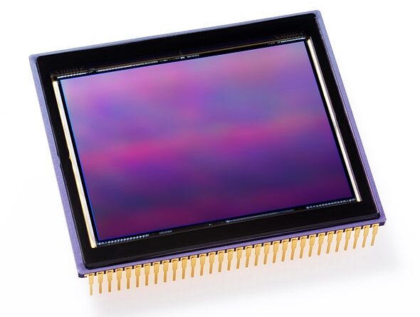
| Photo: Getty Images/DeadDuck |
Nobu Teranishi, Albert Theuwissen and Eric Fossum, who between them made key breakthroughs in the development of both CCD and CMOS sensors, have collaborated on an article for the open-access “Annual Review of Vision Science” journal.
The article: “Digital Image Sensor Evolution and New Frontiers” takes a look back at the significant improvements in sensor technology and the hurdles that each one overcame.
Understandably, it’s quite a technical read, having to describe challenges of both engineering and physics in an article that covers nearly 60 years of developments.
The article touches on details such as the Bayer filter and microlenses, as well as design improvements at the silicon level.
In doing so, it helps explain why we’ve seen the changes in technology that we have.
“CCD technology can be seen as a special, dedicated technology developed and optimized for imaging,” the authors say, but the costs and restrictive yields this brought prompted a push to be able to manufacture sensors using mainstream microelectronics technology.
Click here to read the full article
CCD to CMOS
As the article makes clear, the need to transfer the charges from pixel-to-pixel before they could be read out made it difficult to design faster or higher pixel-count sensors and was challenging to fabricate. It’s hard to imagine the high resolutions and responsive live view and AF systems we have today, had technology continued to iterate on CCD designs.
The article also hints at the timelines involved in these developments, with the first active pixel CMOS designs being created from CCD underpinnings at NASA’s Jet Propulsion Laboratory in 1993 and appearing in Canon DSLRs just seven years later. The camera phone was the “killer app” for CMOS, as it demanded the low power consumption and small size that CMOS offered. The boom in demand for smartphones “supercharged” the development of CMOS, and the world’s largest sensor maker, Sony Semiconductor, stopped making CCD designs in 2015, a little over a decade after the active pixel CMOS chip had been created.
Stacked CMOS
As we approach the present day, the article suggests that Stacked CMOS designs with complex on-chip analog-to-digital conversion could help overcome some of the bottlenecks that otherwise prevent the development of high-speed, high-resolution sensors.
What’s next?
The authors go on to summarize the areas of imaging that are currently pushing sensors forward (including the need for high DR video with no motion artifacts or sensitivity to flicker for autonomous vehicles), and the technologies being pursued beyond conventional photodiode designs. These include Single Photon Avalanche Detectors (SPAD) and the Quanta image sensors that Fossum is working on. It also looks forward to the possibility that technologies such as color routers could allow us to move on from the Bayer design that only captures a single color at each location.
The authors stress the downsides of imaging sensors becoming ubiquitous, but as photographers, their work and those of their colleagues in both industry and academia, have changed our world hugely.
This article was brought to our attention by one of the article’s authors, CMOS pioneer and forum regular Eric Fossum, now a professor at Dartmouth College. Fossum was awarded the National Medal of Technology and Innovation at the White House earlier this month.